Testing Solar Panels V Vs I Curve Reverse Bias

I V Characteristic Of Pv Cell In Reverse Biased Region Download Scientific Diagram
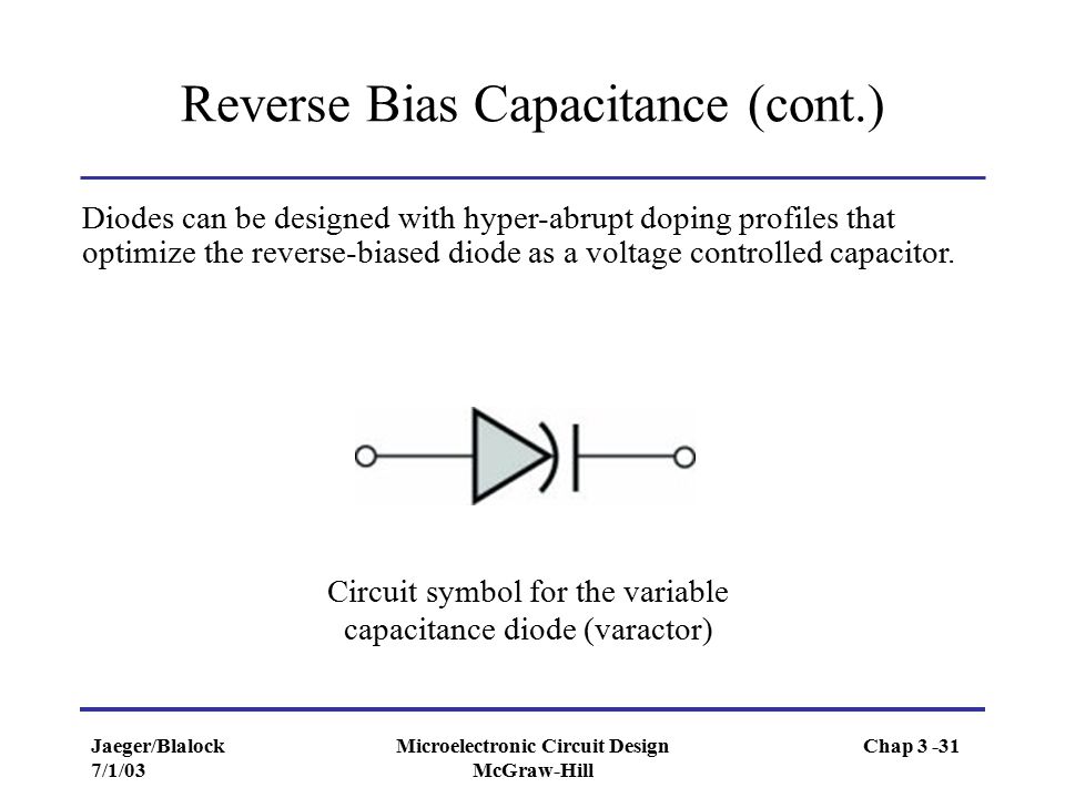
Diodes Learn Sparkfun Com

Pdf Reverse Bias Behavior Of Halide Perovskite Solar Cells

Zener Diode As Voltage Regulator Tutorial

Reverse Bias Behavior Of Halide Perovskite Solar Cells Bowring 2018 Advanced Energy Materials Wiley Online Library
Https Www Mdpi Com 1996 1073 11 9 2416 Pdf

How to test a 12 volt solar panel vs other voltages.
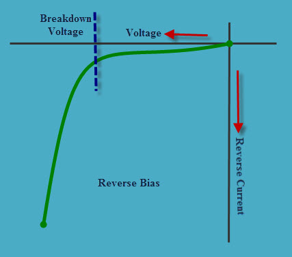
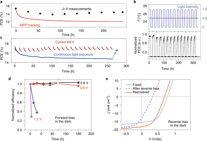
Testing solar panels v vs i curve reverse bias. Figure 1 shows a typical i v curve the power voltage or p v curve that is computed from it and key points on these curves. A solar cell or panel is connected to an smu as shown in figure 6. A four wire connection is made to eliminate the effects of the lead resistance. If your solar cell is a semiconductor diode such as pn silicon cell or pin thin film you get common diode i v curve in dark condition.
One method for determining the shunt resistance of the pv cell is from the slope of the reverse biased i v curve as shown in figure 5. Testing the 12 volt solar panel. Similarly the open circuit voltage voc is the potential that develops across the terminals of the solar cell when the external load resistance is very large figure 3. A linear sweep of the output voltage with a duration of 20 ms was applied in both the forward direction from short to open circuit and the reverse direction.
The topmost figure shows uncorrected i v curves corresponding to a high efficiency solar cell with an open circuit voltage of 720 mv. A solar cell or panel is connected to an smu as shown in figure 6. A larger fill factor is desirable and corresponds to an i v curve that is more square like. At the knee of a normal i v curve is the maximum power.
Typical fill factors range from 0 5 to 0 82. Simply touch the solar panel leads with the multi meter probes matching their corresponding polarity red to red black to black. Fill factor is also often represented as a percentage. Some exceptions may apply based on panel type.
As most solar panels are 12 volts the solar panel test methods are basically the same. There is bigger current in case of forward bias than in. Referring to figure 1 the span of the i v curve ranges from the short circuit current isc at zero volts to zero current at the open circuit voltage voc. Efficiency η efficiency is the ratio of the electrical power output p out compared to the solar power input p in into the pv cell.
You will want to ensure that you place the positive to positive and negative to negative when attaching your multimeter to the connection on the back of your solar panel. A four wire connection is made to eliminate the effects of the lead resistance.

V I Characteristics Of P N Junction Diode

I V Characteristic Curves Or Current Voltage Curves
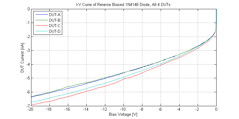
1n4148 Reverse Bias Leakage Current 2n3904blog
Schottky Diode Or Schottky Barrier Semiconductor Diode
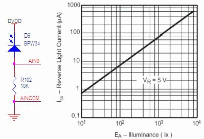
Measure Light Intensity Using Photodiode
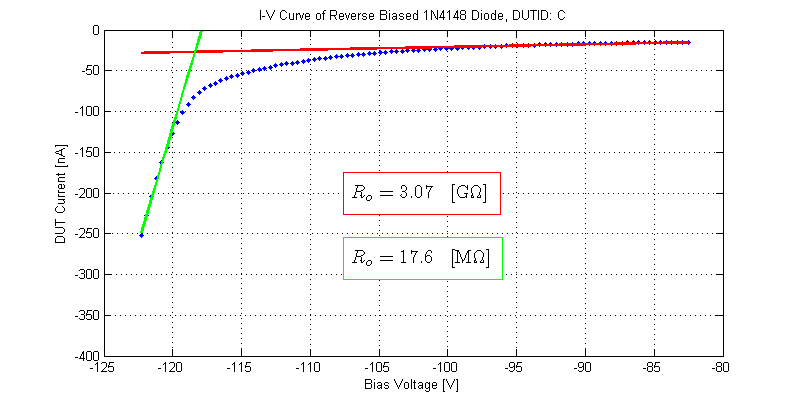
1n4148 Reverse Breakdown Voltage 2n3904blog

Pn Junction Diode Explained Forward Bias And Reverse Bias Youtube

To Draw The I V Characteristic Curve Of A P N Junction In Forward Bias And Reverse Bias Learn Cbse
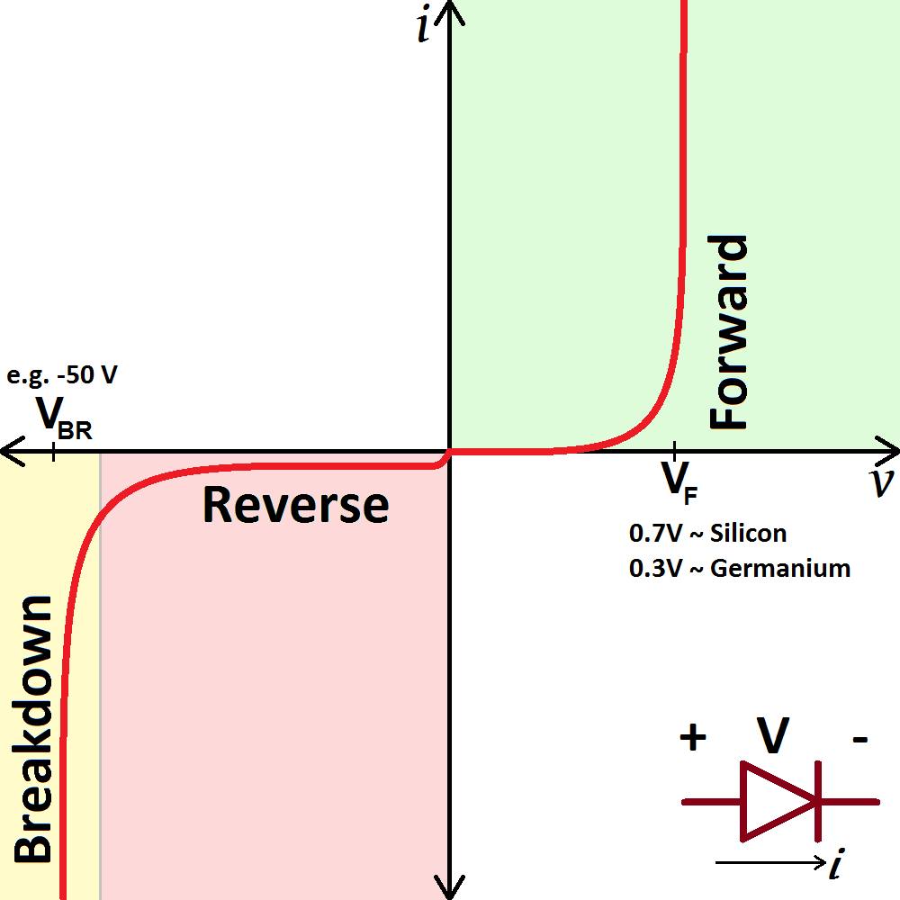
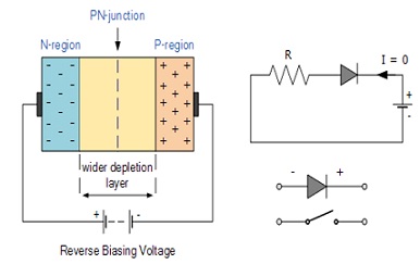
P N Junction Diode Baising And Its Vi Characteristics
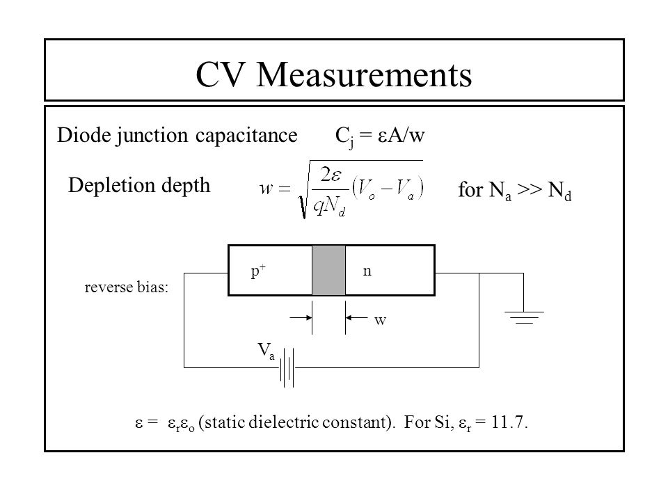
Cv Measurements Diode Junction Capacitance C J A W Depletion Depth Np P W Vava Reverse Bias R O Static Dielectric Constant For Si R Ppt Download

Forward Bias Reverse Bias Diode Working Animation Diode Depletion Region Reverse
Vi Characteristics Of Pn Junction Diode In 3 Biasing Modes
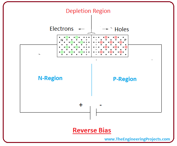
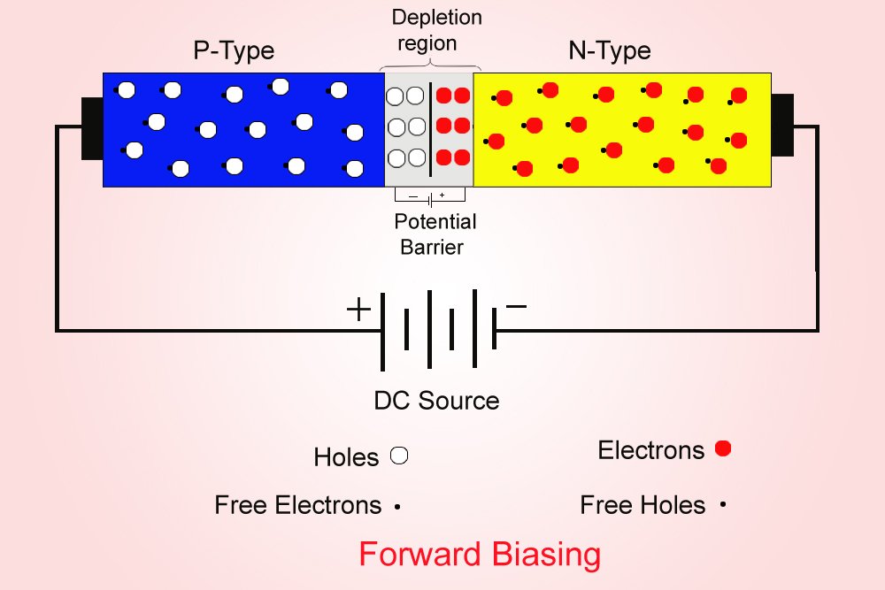
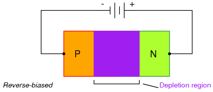
Introduction To Pn Junction The Engineering Projects

Rectifier What Is Rectifier Types Of Rectifier

Outline Chap 1 Introduction Chap 2 Basics Of Semiconductor Physics Ppt Video Online Download

Sensors Free Full Text P N Junction Photocurrent Modelling Evaluation Under Optical And Electrical Excitation Html

Pdf Effect Of Solar Cells Reverse Biased Voltage On Pv Modules Partial Shade Performance

Special Purpose P N Junction Diode Zener Diode Optoelectronic Devices
Https Encrypted Tbn0 Gstatic Com Images Q Tbn 3aand9gctav0nmpzhclr71hkuczehghcl6hu Vbux9xpac9khs1jfwmijr Usqp Cau
Zener Diode Definition Construction Working And Principles
Difference Between Photodiode Phototransistor With Comparison Chart Circuit Globe

Diode Introduction Spinning Numbers
Lessons In Electric Circuits Volume Iii Semiconductors Chapter 3
Consensus Statement For Stability Assessment And Reporting For Perovskite Photovoltaics Based On Isos Procedures Nature Energy

Tunnel Diode Diode Application Tunnel
Types Of Diodes Functional Diagram Working And Characteristics

Reverse Polarity An Overview Sciencedirect Topics

What Is Zener Diode Working Principle Of Zener Diode Electrical4u
Mounted Photodiodes

Schottky Diode Definition Symbol Working And Applications Diode

How Does A Diode And Led Work Eagle Blog

Diodes Everything You Wanted To Know And More

Static And Dynamic Characterization Of P N Junction Solar Cells Sciencedirect
Learn Forward And Reverse Characteristics Of A Pn Junction Diode Meaning Concepts Formulas Through Study Material Notes Embibe Com

Pn Junction An Overview Sciencedirect Topics

Output Characteristic V I Curves Of Junction Fet Electronics Basics Electronic Engineering Transistors

Stability Of Dye Sensitized Solar Cell Under Reverse Bias Condition Resonance Raman Spectroscopy Combined With Spectrally Resolved Analysis By Transmittance And Efficiency Mapping Sciencedirect

Photodiode Circuits Operation And Uses
Topic 3 Diodes And Diodes Circuits Ppt Download

Photodiode Basics Wavelength Electronics
Schottky Diode Working Characteristics Applications

Varistor Symbol And Applications Electronics Projects Electrical Projects Electronics